Nanometer CMOS ICs Statistical Analysis: Application to Design and Test (ANESPA)
Technology scaling has surpassed the 100nm barrier and is now rapidly evolving to the 65nm technological node. One of the main challenges of today’s technology scaling is related to controlling geometric critical dimensions, not only from die-to-die, but also within the die. The impact of poor critical dimensions control results in parameter variations of devices and interconnect. Recent results point that the relative impact of within-die variations is of the same order than die-to-die variations and have a significant impact on present design and test methods, since many of the physical-to-electrical relationships at the circuit level are not deterministic anymore. This poses important challenges in specific design steps (like critical path determination) and impacts the development of efficient test methods based on non-logical parameters. This is motivated by two main reasons: the lack of appropriated models to describe variation, and the difficulty in settling pass-fail limit regions in a noisy environment. The first factor has an impact on the development of appropriated design and test methods that must rely on worst-case design techniques.
The objective of this project is the development of efficient statistical models for the key circuit parameters (design, power, and temperature), and the development of parametric test methods (mainly related to delay fault and current-based techniques) where the pas/fail region limit is settled according to such statistical models. Another objective of the project is to include the impact of noise mechanism and environmental fluctuations (temperature and supply voltage) in the models to describe their effect on variation.
This project started on January 2006, the main expected results are in the following areas:
We will investigate the impact of variations on the main circuit parameters and will develop accurate models to capture their dependence.
Some preliminary results show such an impact on:
Figure shows the static power dissipation at the circuit level considering statistical variations in channel length, substrate doping and gate oxide thickness.
Additional detailed results will be presented in PATMOS'06 to be held next September
We are currently investigating different design techniques that will help in reducing both static and dynamic variation components on delay and power
Parameter variations have a significant impact on test methods. We investigate these relationships to develop advanced strategies suitable of being applied in sub-90nm technologies.
We are currently analyzing in detail some correlation techniques to determine the impact of parameter variations.
Delay testing at low-VDD has been proposed as a useful test method to expose delay defects not detectable at nominal supply voltages. The advantage of this technique comes from the reduced transistor strength at lower supply voltages that increases the impact of delay defects in faulty circuits with respect to the fault-free population. The correlation between the supply voltage and the delay, founded on the well-known relationship between these two circuit parameters, is used to set the delay limit according to each supply voltage value. Less attention has been given to the impact of supply voltage reduction on the circuit parameter variation dependency and its impact on the delay distribution. We investigate this relationship and found that for a 130nm technology the delay variations are worsened when lowering the supply voltage from the nominal 1.2V to 0.9V by more than 80%. This dependence may question the advantage of Low-VDD vs. delay testing for future nanometer technologies.
The root cause for this is illustrated in the Figure where the delay (y) vs. Vdd (x) curve shows that the same amount of VT variation translates to a much higher delay variation at low VDD values with respect to the nominal voltage.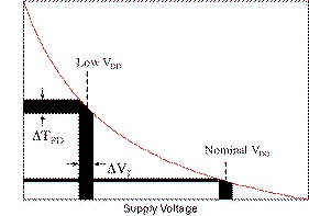
Additional results and more details can be found in the Proc. of the 24th IEEE VLSI Test Symposium, 2006.
C. Hawkins, P. Zarkesha-Ha, J. Segura
13th NASA Symposium on VLSI Design - Post Falls, Idaho, June 5-6, 2007.
The electronic focus in integrated circuits has evolved from major attention to the transistor to an equal concern with the interconnect metal. Modern ICs have evolved to many levels of metal with total wire length on the order of miles. Scaling brought many performance and cost advantages but also brought us to the limits of manufacturing these metal systems without serious defects. The majority of these metal defects are not the classic bridge or open types, but the difficult to detect resistive vias. This paper describes the problems, and then shows the reliability risk of the via defects that can easily escape the test process.
B. Alorda, J.Caubet, M. Cañellas, I. de Paúl, S. Barcelo, S. Bota and J. Segura
XXII Design of Circuits and Integrated Systems Conference (DCIS’08)
We present a tool that computes the charge delivered to a combinational circuit when a given set of test vectors is applied. It is thie first component of a more complete suit oriented to determine and evaluate the coverage of a test vector set developed for Charge Based Testing (CBT). The tool estimates the circuit internal activity and computes the charge delivered. Results from data obtained using 130nm fabricated ICs are provided.
J. Rosselló, C. de Benito, S. Bota and J. Segura
Lecture Notes in Computer Science, 4148, 66-74, 2006.
We present a novel technique to accurately describe the leakage power in CMOS nanometer Integrated Circuits (ICs) considering process variations. The model predicts a leakage power increment due to process variations with high accuracy. It is shown that leakage increases considerably as channel length variations become larger due to technology scaling. The present work also describes accurately the dependence of leakage dispersion with process variations. The model developed shows that, even if channel length variations are kept small the leakage dispersion is considerably large. Finally, the concept of “Hot Gates” (HGs) is introduced, showing that HGs will be an important re-liability factor in near future nanometer technologies.
J.L. Rosselló, C. de Benito, S.A. Bota, J. Segura
Design Automation and Test in Europe (DATE 2007)
As CMOS IC feature sizes shrink down to the nanometer regime, the need for more efficient test methods capable of dealing with new failure mechanisms increases. Advances in this domain require a detailed knowledge of these failure physical properties and the development of appropriated test methods. Several works have shown the relative increase of resistive defects (both opens and shorts), and that they mainly affect circuit timing rather than impacting its static DC behavior. Defect evolution, together with the increase of parameter variations, represents a serious challenge for traditional delay test methods based on fixed time delay limit setting. One alternative to deal with variation relies on adopting correlation where test limits for one parameter are settled based on its correspondence to other circuit variables. In particular, the correlation of circuit delay to reduced VDD has been proposed as a useful test method. In this work we investigate the merits of this technique for future technologies where variation is predicted to increase, analyzing the possibilities of detecting resistive shorts and opens.
B. Alorda, I. de Paul and J. Segura
IET Computer Digital Technology, 1 (5), pp. 481-490, 2007.
A BIST architecture is presented to perform charge-based testing (BIST-CBT) on embedded memories where direct access to I/Os is limited. The proposed architecture includes a charge monitor, a functional test algorithm generator (that applies a standard March B algorithm) and output processing circuitry. The method is based on a charge correlation technique validated experimentally on previous works for submicron SRAMs. The testing methodology implementation has two phases: a short pre-characterisation phase performed during manufacturing test to ensure process-variation immunity, and the actual BIST-CBT. Data from the first phase are processed and loaded in the BIST circuitry registers. The proposed embedded BIST circuitry provides a digital output pass/fail flag that signals the result of the functional and BIST charge analysis (both based on the same March algorithms). To demonstrate the viability of the proposed architecture, a prototype is designed that has been implemented in two parts: the charge monitor is the core of the BIST circuitry, and has been developed in 120 nm CMOS technology, whereas the digital processing circuitry has been implemented on a FPGA device.