Multipar Test Methods for Nanometer IC Technologies (Multipar)
Test Methods for Nanometer IC Technologies
Scaling advanced CMOS technology to the next generations improves performance, increases transistor density, and reduces power consumption. As a result of a constant device and interconnect scaling, current CMOS technology processes are below the 100nm range, and are referred to as nanometer technologies. One drawback of technology scaling is related to process parameter fluctuations. Parameter fluctuations in nanometer technologies come from poor control of critical dimensions and doping profiles, impacting geometric and electrical parameter distribution as the MOSFET transistor voltage (Vt), the off-state current (Ioff), and the saturation current (IDsat). Recent studies point that parameter fluctuation will have a significant impact on IC test and verification effectiveness in nanometer technologies.
The objective of this research project is to analyze the impact of parameter variation on the IC behavior, and to include this source of circuit malfunction into the test flow through specific compact fault models. The main goal of the research plan is to develop a new test technique based on correlating multiple parametric test observables to predict circuit integrity. This is required since parameter variations limit the effectiveness of single-parameter non–logic based test methods due to the difficulty to establish golden reference values. We will investigate the merits of a multi-parameter based test strategy that correlates a number of circuit parameters (delay, leakage current, active energy, temperature variation, etc.), to distinguish between faulty and fault-free circuits. The project is built on the basis of technology transfer to industry and incorporates tasks oriented to develop CAD modules and also specific circuit monitors to capture the parametric observables considered.
The main properties are:
- The charge is related only to the gates having activity and can be applied at-speed. This allows an efficient verification of large circuits as internal blocks can be selectively tested by inducing higher activity in these parts, while minimizing activity in the remaining parts.
- The charge contains both static and dynamic power components, although depending on the measurement technique, the static component can be neglected thus enhancing the resolution related to the circuit activity.
- The correspondence between circuit activity and charge delivered to the circuit makes it possible to locate the fault site by proper correlation between these two variables.
The development of circuit monitors is of high importance since automatic test equipment (ATE) has limited compatibility with non-logic parameters, thus limiting the implementation of the proposed technique in production environments.
The IC transient current can be measured either from outside the circuit or internally.
Given the challenges related to capture consistently the transient supply current, we developed a specific circuitry to be placed between the circuit and any standard measurement setup like the load board of an ATE. The structure of the monitor is shown in the figure: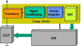
The last implementation of the off-chip module (CHARDIN) is shown below
A 130nm version of a buil-in monitor has been fabricated. The main characteristics are:
- 1.41GHz Bandwidth
- 3230V/μs Slew rate (1V Step)
- 21.43 dB CMRR
- 1.59ns Settling time (1V step)
A non-invasive interface for the built-in version has been designed and fabricated. The principle of operation is illustrated in the figure: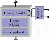
We have developed several alternatives to extract circuit information from charge correlation to explore the possibilities of getting pass/fail information directly from the charge data. Data shown comes from commercial memories provided for these experiments.
Charge vs. memory address for a fault-free memory
Charge vs. memory address for a falty memory
Charge vs. memory cell position witin a memory block for a fault free memory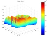
Charve vs. memory cell position within a memory block for a faulty memory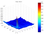
S. Bota, M. Rosales, J. Rossello, J. Segura
IEEE VLSI Test Symposium, 2006
Delay testing at low-VDD has been proposed as a useful test method to expose delay defects not detectable at nominal supply voltages. The advantage of this technique comes from the reduced transistor strength at lower supply voltages that increases the impact of delay defects in faulty circuits with respect to the fault-free population. The correlation between the supply voltage and the delay, founded on the well-known relationship between these two circuit parameters, is used to set the delay limit according to each supply voltage value. Less attention has been given to the impact of supply voltage reduction on the circuit parameter variation dependency and its impact on the delay distribution. In this work we investigate this relationship showing that for a 130nm technology the delay variations are worsened when lowering the supply voltage from the nominal 1.2V to 0.9V by more than 80%. This dependence may question the advantage of Low-VDD vs. delay testing for future nanometer technologies.
J.L. Rossello, C. De Benito, J. Segura
IEEE Trans. On Circuits and Systems II: Express Birefs, Vol. 52, No. 10, pp.685-689, Oct. 2005.
We present an accurate model to estimate the energy and delay of domino CMOS gates derived from a detailed description of internal capacitance switching and discharging currents. The delay dependence with the position of the switching transistor in the gate is accurately described with the advantage that it does not include additional empirical parameters, thus providing the propagation delay in terms of foundry-provided MOSFET parameters. Results show a very high accuracy with a relative error lower than a 3% with respect to HSPICE for a 0.18Pm CMOS technology providing up to three orders of magnitude of speed improvement. The analytical nature of the model makes it suitable for circuit optimization and is the basis for a quick estimation of ULSI circuits power and delay when used in circuit simulation tools.
J. L. Rossello, and J. Segura
IEEE Trans. On Circuits and Systems I: Regular Papers, Vol. 51, No. 7, July 2004.
We develop an accurate analytical expression for the propagation delay of submicrometer CMOS inverters that takes into account the short-circuit current, the input–output coupling capacitance, and the carrier velocity saturation effects, of increasing importance in submicrometer CMOS technologies. The model is based on the th-power-law MOSFET model and computes the delay from the charge delivered to the gate. Comparison with HSPICE level 50 simulations and other previously published models for a 0.18- m and a 0.35- m process technologies show significant improvements over previous models.
B. Inıguez, J.P Raskin, P. Simon, D. Flandre, and J. Segura
Solid-State Electronics 47 (2003) 1959–1967
Silicon-on-insulator (SOI) is emerging as a strong technology candidate for low-power high-performance applications. In this work, based on experimental data, we review the fundamental aspects of leakage current in deepsubmicron SOI CMOS technologies discussing the underlying physical mechanisms and their dependence with bias, temperature and operating frequency. These mechanisms and their evolution with technology scaling are compared to those of bulk CMOS. Subsequently, we evaluate the merits of parametric IDDX testing techniques based on current monitoring when applied to these technologies.
B. Alorda, V. Canals, J. Segura
Journal of Electronic Testing: Theory and Applications, 20, pp. 543-552, 2004
We evaluate the possibilities of transient current testing practical implementation by comparing the transient supply current signature at the IC supply pins to its internal behavior. This analysis is key to correlate the internal circuit block transient current shape to the waveform measured outside the IC. These waveforms may differ significantly due to the power supply grid, whose capacitive and inductive components can modify both the frequency and magnitude components of the transient current. Given the complexity of today ICs, an accurate description of the circuit power grid is required to investigate the merits of transient current testing (idd(t)) approaches. In this work we develop and analyze a hierarchical power-grid equivalent circuit to evaluate the supply current frequency components and their distribution over the power/ground grid hierarchy. This is a key step to determine the feasibility of on-chip vs. off-chip idd(t) strategies and their posterior application to on-line testing.
J. Altet, J. Rosselló, A. Rubio and J. Segura
IEEE Communications Magazine, Vol. 41, No.9, pp. 98-104, September 2003
Current RFIC test practices perform systemlevel verification through specific functional validation. Structural testing, although widely accepted for digital and analog generic ICs, is not adopted in this domain due to the lack of appropriate fault models. Another important reason is the impossibility of embedding testmode circuitry within the RF blocks because of parasitic component disturbances. This work discusses the feasibility of complementing functional tests with structural methods by using thermal testing. The benefits reside in the intrinsic electrical loadless property of the technique and the impact of many defects on the circuit temperature. The analysis focuses on the possibilities of detecting defects that escape functional testing, and practical implementation issues.
B. Alorda, B. Bloechel, A. Keshavarzi, and J. Segura
IEE Electronics Letters, Vol. 38, No. 18, pp.1028-1029, 2002
An off-chip monitor is presented that measures the transient supply current of CMOS ICs and provides the charge delivered to the circuit. The monitor is designed to be placed on the automatic test equipment board fixture and automate transient current supply testing. Experimental results demonstrate up to 1 GHz bandwidth operation.
J. Rosselló and J. Segura
IEE Electronics Letters, Vol. 38, No. 15, pp. 772-774, 2002
A simple method to evaluate the propagation delay of complex CMOS gates computed from inverter delay models based on the nth-power law MOSFET model is presented. The method is based on a transistor collapsing technique developed for complex gates and takes into account short-channel effects, internal coupling capacitances and the body effect. The propagation delay of complex gates for a 0.18 mm technology is evaluated, showing excellent results.
J. L. Rosselló and J. Segura
IEEE Transactions on Computer Aided Design of Integrated Circuits and Systems, Vol. 21, No. 4, pp.433-448. 2002
The authors present an accurate analytical method for analyzing the power consumption in CMOS buffers. It is derived from the charge transferred through the circuit and makes use of the physically based MM9 MOSFET model (Velghe et al., 1994), (Foty et al., 1997) as well as a modified Sakurai alpha-power law model. The resulting analytical model accounts for the effects of input slew time, device sizes, carrier velocity saturation effects, input-to-output coupling capacitance, output load, and temperature. Results are compared to HSPICE simulations (level 50) and to other models previously published considering a large set of parameters for a 0.18 and 0.35 m technologies, showing significant improvements
B. Alorda, V. Canals, I. de Paul and J. Segura
IEEE International On-Line Testing, 2004 (IOLTS)
Abstract:We present a BIST architecture to perform Charge Based Analysis on embedded memories. The architecture includes a charge monitor as well as the input generation and output processing circuitry. The method applies a charge correlation technique validated experimentally on previous works for submicron SRAMs. The technique requires a short pre-characterization phase during manufacturing testing that guarantees process-variation immunity. The embedded BIST circuitry provides a digital output pass/fail flag that signals the result of the BISTcharge analysis.
B. Alorda and J. Segura
IEEE Int. On-Line Testing Symposium, France, July 2005
We propose and evaluate a non-intrusive built-in monitor oriented to transient current based testing of digital CMOS VLSI circuits. The monitor measures the transient current idd(t) by sensing the voltage drop at an inductance coupled to the magnetic field produced by the power supply transient current. Designed in 120nm CMOS technology, the sensor proposed has two blocks. The transducer circuit senses the transient current and provides a voltage waveform, while a second module amplifies the voltage waveform and computes the transient current waveform Idd(t) to produce the charge waveform. Simulation results, using an elaborated CUT model, demonstrate the performance of the new transceiver element.